
FER-403 GaN pd35W Resolution
author: shim
2022-11-14
ANALYSIS OF FERPOWER'S DUAL USB-C GaN CHARGER
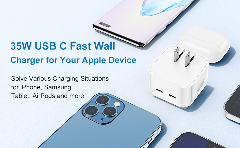
The charger is designed with white squares for a small and sophisticated look and has its own folding pins for easy everyday use. The charger has 35W output power, and the output supports blind plugging, which can not only meet the charging needs of mobile phones; but also charge laptops, the following will be analyzed to see how the design of the charger is inside.
35W gallium nitride charger
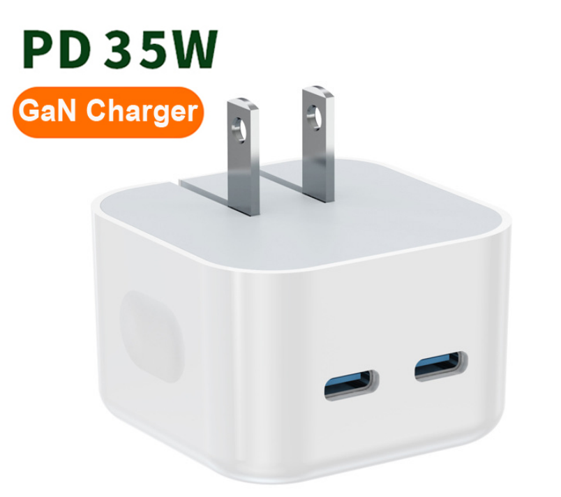
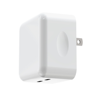
The charger adopts a white PC case, the surface is mirror-polished, the top surface is slightly convex and the edge is angled.
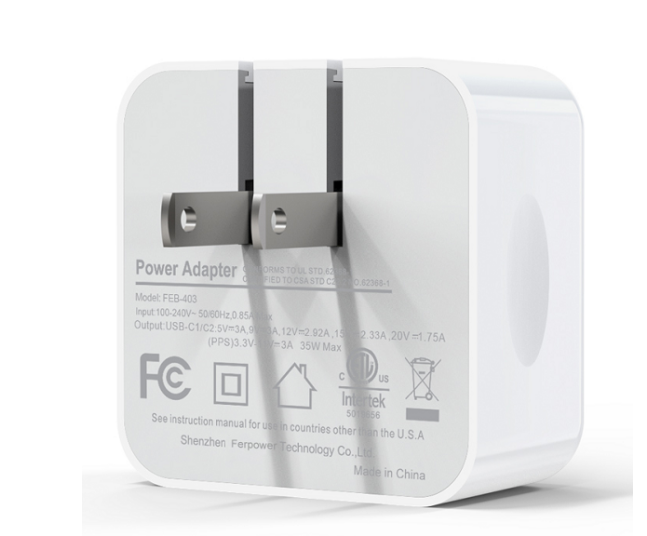
The input housing is printed with the charger parameter
model:FEB-403;
Input:100-240V~50/60Hz 1AUSB-C1/C2
Output:5V3A、9V3A、12V2.92A、15V2.33A、20V1.75APPS:3.3-11V3A
Total Output:35W Max
Certificate: ETL/FCC/PSE/CE/UKCA/SAA/RCM/C-TICK
model:FEB-403;
Input:100-240V~50/60Hz 1AUSB-C1/C2
Output:5V3A、9V3A、12V2.92A、15V2.33A、20V1.75APPS:3.3-11V3A
Total Output:35W Max
Certificate: ETL/FCC/PSE/CE/UKCA/SAA/RCM/C-TICK
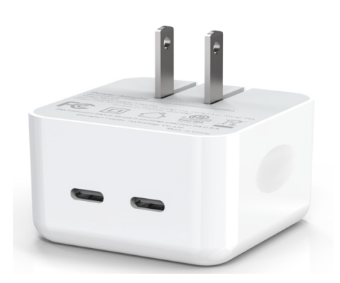
The charger is equipped with foldable US standard pins, which are easy to store and carry.
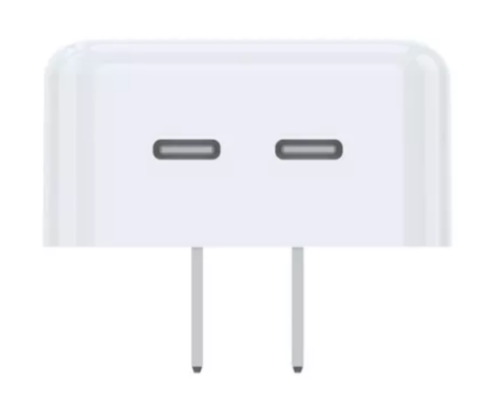
The other end is equipped with dual USB-C ports,
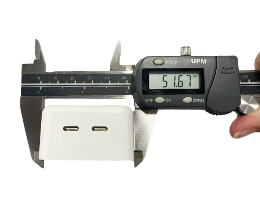
The height of the charger body was measured to be 51.70mm.
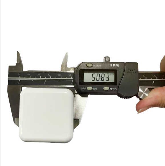
The width is 50.80mm。
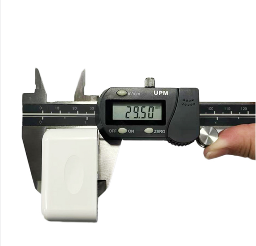
The thickness is 29.50mm。
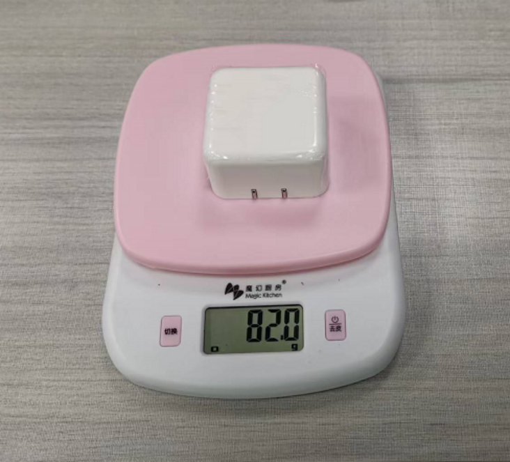
In addition, the net weight of the charger was measured to be about 82g。
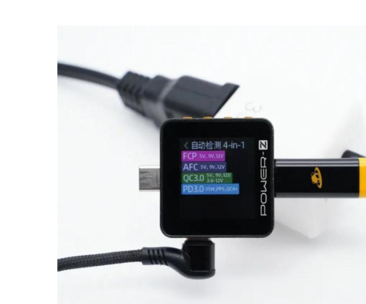
Using ChargerLAB POWER-Z KM002C measured USB-C1 port supports FCP, AFC, PD3.0, PPS, charging protocols.
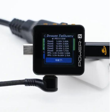
And it has five sets of fixed voltage gears of 5V3A, 9V3A, 12V2.92A, 15V2.33A, 20V1.75A, and two groups of PPS voltage ranges of 3.3-11V3A and 3.3-16V2.15A.
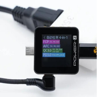
The C2 port compatibility protocol is exactly the same as that of C1 port.
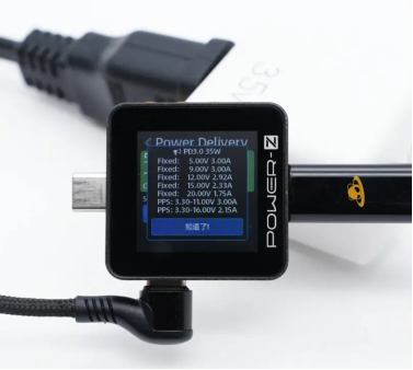
The PDO message is also identical, the performance of the two C-port single-port outputs is exactly the same, and the power blind mating is supported.
How about the materials and workmanship of the interior.
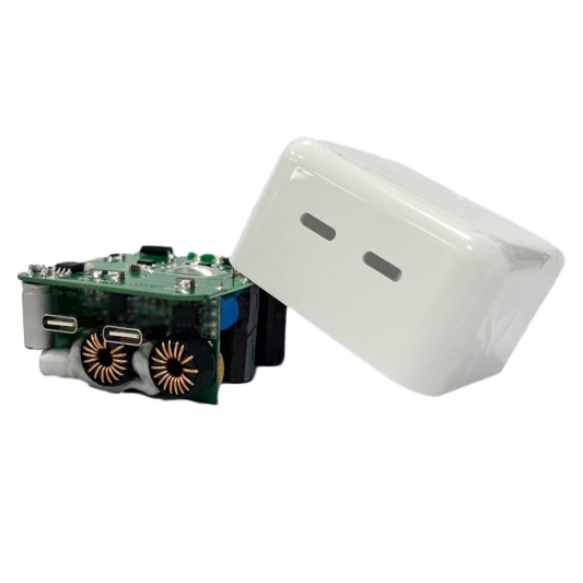
First, pry the shell along the seam of the charger housing, glue and fix the inside of the PCBA module, and connect the folding pins to the PCBA module through shrapnel.

The inside of the charger is fixed with white glue for primary and secondary step-down plate insulation. The front of the PCBA module is at a glance, and the left side of the welded input board, capacitor, and transformer are all glued and reinforced. The lower soldering buck plate, the small board soldering buck inductor, buck chip, USB-C socket, etc.

Tow of the filter capacitors is 33μF 400V.
In the middle of the two capacitors is a differential-mode inductor, which is insulated by a heat shrink tube.
storage power supplies and other aspects.

One of the external power supply capacitors is 560μF 25V.
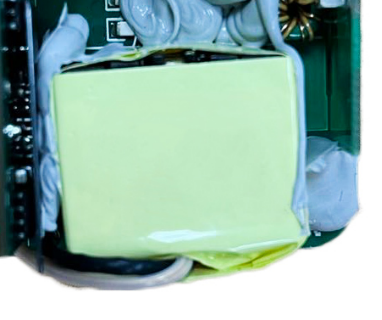
The transformer core is tightly wound and insulated with tape。
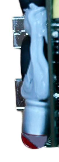
The buck board is welded at the output end of the charger, and the buck inductor and output filter capacitor are also soldered on the small board, and the components are glued and fixed.

Remove the buck plate, and solder two protocol chips, two buck inductors and two output filter capacitors to the front of the board, both of which have the same design.
Select one of the ways to introduce it.
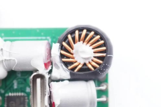
The buck inductor jacket heat shrinkable tube is insulated and glued to fix.
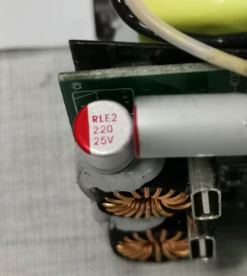
Output filter capacitor specified as 220μF 25V.
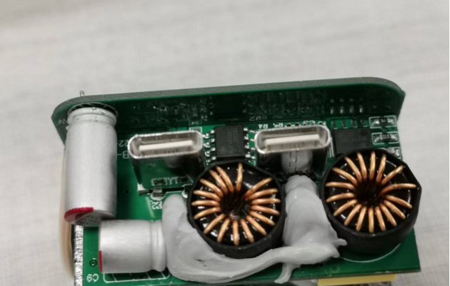
The USB-C female base is fixed with vias soldering, and the white rubber core does not expose copper